


Key takeaways:
- What used to be secondary, independent physical effects in semiconductor design are becoming primary and interdependent with 3D-Integrated Circuits (3D-IC) chips and reuse of IP chiplets.[1] Moving from the scale of silicon to system requires an integrated suite of design, simulation, and analysis tools which comprehend the combined multi-physics effects, thereby improving design understanding and decision making across multiple engineering domains (EDA, MCAD, MCAE).
- The cost and delays due to design re-spins as silicon manufacturing ramps up are unacceptable given the exploding bespoke IC market. Design understanding gained via multi-physics performance simulation and analysis with no compromise in accuracy is crucial as 3D-IC / System on a Chip complexities and volumes increase.
- Automatically and continuously proving functional safety to meet industry standards such as ISO 26262 during custom chip design and packaging for new products that rely on more embedded software is critical for an OEM’s future product success.
- Ansys is a proven leader in simulating mechanical, electromechanical, thermal, and radio transmission, predicting unwanted multi-physics interactions—noises, vibrations, physical interferences, and material fatigue all leading to system failures.
- Ansys provides essential expertise across the scale of tomorrow’s cyber-physical products—understanding silicon engineering workflows as well as system engineering workflows and everything in between to create an innovative and profitable product.
Thanks to Moore’s Law, computing continues to decrease in unit costs making it easier to add new features, even during product use well after mass production. Products in all industries are increasing their dependence on electronics and software functionality including being connected as “smart” Internet of Things (IoT) devices. With embedded software, electronics, and more sensing, innovative value streams will be discovered and developed where simulation, analysis, and data science are required skills throughout product design. This new way of providing a product, as a set of applications on a computing platform, is also driving IC demand.[2]
The computer aided engineering tools and practices originally used to improve mass production of mechanical things, then electro-mechanical things, are now needed to design miniature IC devices. IC system designers will take advantage of stacking chiplets in various 3D packages while managing power use, data pre-processing at the sensor, and durability while also avoiding electromagnetic interference.
The design and development of complex cyber-physical systems requires well integrated capabilities for cross-disciplinary simulation, analysis, and design optimization. Ansys provides a broad and revenue-leading platform for multi-physics simulation and improved understanding for many mechanical, optical, and electrical based products.[3] As the semiconductor industry moves beyond mostly planar designs and manufacturing, they will need this expertise to design, evaluate, and certify that a new 3D-IC is ready to be manufactured, especially in times of semiconductor foundry under capacity.
Emergence of 3D-IC in Systems Driving Need for Changes
Electronics content in end products continues to increase. Providing more value for less money driven by continued integration and greater capability. Sensors can be integrated with their connected digital elements. Integration of digital components on a single substrate is exposing coupled physical phenomena which must be understood when developing robust systems.
Real estate management on the silicon wafer is now encouraging the use of the vertical dimension leading to new 3D-ICs. This emergence of the 3D-IC is also driven by reused or purchased intellectual property (IP) modules. Three dimensional designs provide packaging engineers more options as they manage communications, thermal, and power distribution. Interestingly, these issues are similar to those found in architecture, engineering, and construction (AEC) for building and facility designs, with different constraints for physical packaging and coupling. Managing air flow for breathing, heating, and cooling within a building requires thermal simulation capabilities. Wiring for networks and wiring for power grids need to be packaged in a building to not interfere with each other. Both produce some heat, based on the electronics installed and thus the overall building design and construction is developed by engineering balancing all of these performance criteria. Consider EMI/EMC when signals traverse longer distances—they become unintended antennas. Architects & engineers shield these in buildings.
Shielding per se is not sensible with IC miniaturization. New design techniques for assuring signal robustness are required. Innovation will be best supported with coupled EMI/EMC/power flow simulations. Once a power grid is designed then thermal management must be confirmed. Utilizing the vertical dimension greatly improves the signal robustness by shortening communication paths.
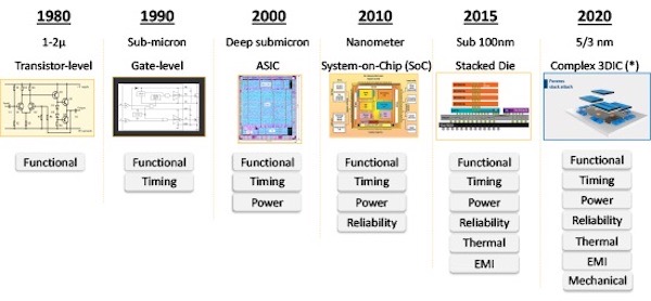
Figure 1—Increasing Integrated Circuit on a Chip Challenges[4]
Figure 1 summarizes the electronics industry’s journey and its technological demands over the past four decades. Just like the advances in packaging for cars and buildings—EDA needs to embrace more simulation capabilities and in a multi-physics platform. This demand will continue to increase as markets continue to demand more features faster and cheaper. The EDA tools must help electronics and systems engineers deliver proven designs. Re-spins in the IC prototyping and manufacturing launch are just not acceptable given their extreme cost and delay in time to market.
Key 3D-IC Design Analysis Solution Requirements
CIMdata believes the evolution of traditional semiconductor designs into 3D packages will follow the same journey that other engineering disciplines have followed with coupled physics analyses and multidisciplinary collaborative workflows. Consider examples of thermo-fluid analyses in chemical engineering or aero-mechanical flutter in aircraft design.
Material properties management is necessary to help simulation engineers use consistent, measured characteristics of a material when simulated. A company needs material management to handle traceability and raw material reporting when mass producing a product. In some cases, the material or treatment becomes a key resource which needs to be managed in its own supply chain.
3D-IC chip designers will see the need for improved materials management as they balance design trade-offs. Understanding design weaknesses of any communications, from AM/FM radio to Wi-Fi to internal communications within a product, has required anaerobic test cambers to discover electro-magnetic vulnerabilities. Once any of these phenomena are understood, they can be simulated.
By looking at the trend of chip design failures, the root cause of expensive manufacturing process re-spins can be managed through improved simulation and design exploration. Multi-physics interactions (i.e., thermal driving structural bending) and mixed-mode analog and digital circuits (typical in sensor integration) are growing causes of chip design failures in the past few years.
New areas of failure include demands for cyber-security and safety – which may be achieved with certified IP electronic circuitry. Placing these proven IP chiplets into a new system design still requires a confirmation that thermal and system robustness are achieved. This can and should be confirmed virtually, continuously during development.
Multi-physics problems might be addressed merely by packaging the digital elements in three dimensions. However, some packaging considerations can make certain conditions worse, e.g., heat management. While shrinking the design space and voltage needed can lower heat management demands, this can increase signal integrity issues. Perfecting signal integrity improves enclosing system robustness. Discovering thermal and signal interferences in a prototype is no longer feasible. Requiring a spin of the new silicon design with the intended product configuration (which makes signals more exposed) is too slow in today’s fast to market economies. This must all be done in an integrated system simulation.
In fact, design alternatives could be assessed via figure of merit analyses using multi-physics simulations and multi-disciplinary analysis optimization (MDAO) which consider intended function and thermal/signal robustness. A foundry could require simulation evidence that a design will work, before accepting the design for manufacturing.
Multi-Physics Workflow Automation Requirements
Insights often are discovered collaboratively. They often are a competitive advantage. Figure 2 shows key roles interacting during semiconductors and systems design activities. These activities are done in parallel, not sequentially. Models provide the framework to assess and discover physical interactions and influences.
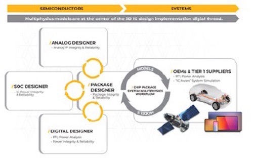
Figure 2—Collaborative Workflow Speeds 3D-IC Invention
It is unrealistic to expect a single solution provider to have all the latest simulation and modeling capabilities spanning all engineering domains. What is key is an open and collaborative environment that facilitates seamless workflows across scales and enables the end customer to leverage best in class practices that integrate with their own internal workflows. The same workflow environment will be used to automate testing as both the silicon and the embedded software are developed by OEMs and TIER 1 suppliers. Continuous Systems on a Chip (SoC) and systems verification and validation will be performed with simulation solutions from Ansys well integrated with other tools as evolving IC technologies change the design requirements.
Ansys’s 3D-IC Design Analysis Solution
CIMdata’s annual S&A Market Analysis Report documents Ansys’ leadership position in the S&A segment.[5] Ansys realizes that efficiently designing complex products requires a focus on manufacturing and robust system designs aided by computer-based engineering tools which accurately predict the multi-physics coupling within systems. Material properties and simulation techniques are at the core of building capable simulation platforms. Ansys has earned its reputation as a go-to CAE applications solution provider where multi-physics coupling must and can be explored. As the challenges of 3D-IC power management, packaging, IP reuse, and new manufacturing techniques are discovered, CIMdata believes Ansys will provide a simulation and material properties backbone to assure first time capable semiconductor designs, just as they have done for decades in the aerospace and automobile industries.
Foundry Certifications
IC foundries exist thanks to Moore’s Law: realizing that smaller geometry in gate design could deliver the same function as thousands of connected transistors. IC foundries are competing to provide IC manufacturing processes for finer and finer geometries. Knowing the physical margins to eliminate expensive redesigns is key to semiconductor manufacturing foundries utilization. Leading IC foundries, TSMC and Samsung, are now requiring evidence of proper thermal and EMC simulation. Here is what they have said about Ansys:
- “The result of our collaboration combining Ansys’ multi-physics solutions and TSMC’s CoWoS® and InFO advanced packaging technologies helps our mutual customers address their design complexity and challenges,” said Mr. Suk Lee, senior director of the Design Infrastructure Management Division at TSMC.[6] The next smaller geometry scale at TSMC, a 3nm IC manufacturing process will require Ansys usage.[7]
- “The certification of Ansys Redhawk-SC, Redhawk, and Totem supports our joint customers in rapidly completing new designs with improved confidence by managing increased power integrity, reliability, and thermal challenges,” said Mr. Sangyun Kim, vice president at Samsung Electronics.[8]
Just like car design’s crash worthiness was demonstrated in LS-Dyna simulations, engineers will evaluate their new 3D-IC designs with simulation runs which include final SoC packaging. Understanding and addressing coupled physics before using IC foundry capacity will become an expected practice.
Concluding Remarks
3D-IC innovation is accelerating. The benefits from pattern matching and pervasive sensing are just starting. New value propositions will continue driving the need for revenue generating feature innovations. As IoT expands, collecting much more data and feeding them into machine learning algorithms, more custom integrated circuits are being developed. The data and computing cloud community is even designing bespoke chips to optimize their artificial intelligence and machine learning (AI/ML) techniques. This will continue to drive IC design architectures into the realm of 3D.
Ansys has assembled a large collection of simulation capabilities used for the last few decades for improving mechanical (e.g., crash simulation and aerodynamics), electro-mechanical (electro propulsion for trains, industrial machinery, and now passenger vehicles), optical, and radio/communication systems (including EMI/EMC, both wired and over the airwaves). This multi-physics design capability is an area where Ansys has offered a leading simulation and analysis solution set for many years.[9] A backbone for product durability is capturing and managing material properties, now including silicon technologies. Ansys’ acquisition of materials management industry leader Granta provides a key backbone. Ansys is now turning their focus to solutions that address the emerging 3D-IC domain.
Ansys knows that coupling between different physical phenomena becomes more complicated in three dimensions and as new load cases are discovered. Their expertise and track record in mechanical and electrical products is well known. They are ready to help chip designers understand the physical couplings as they architect new kinds of 3D-IC layout and packaging.
CIMdata believes Ansys’ application of their proven multi-physics simulation solutions to the 3D-IC design challenges will set the hallmark for SoC design tools enabling complex products in the future. Ansys understands and fosters the importance of systems simulation driven design and manufacturing. Their simulation and modeling capabilities have been expanded to now include electronics, especially 3D-ICs and their resulting SoCs.
[1] https://ieeexplore.ieee.org/stamp/stamp.jsp?tp=&arnumber=9078405
[2] Research for this commentary was partially supported by Ansys.
[3] CIMdata 2021 Market Analysis Report Series Simulation & Analysis Market Analysis Report
[4] https://www.3dincites.com/2020/05/modeling-simulation-and-test-for-multi-die-ic-designs/
[5] CIMdata 2021 Market Analysis Report Series Simulation & Analysis Market Analysis Report
[6] https://www.ansys.com/news-center/press-releases/08-26-20-ansys-multiphysics-solutions-certified-by-tsmc-for-high-speed-next-generation-3d-ic-packaging-technologies
[7] https://www.ansys.com/news-center/press-releases/08-25-20-ansys-achieves-certification-of-its-multiphysics-solutions-for-tsmcs-3nm-process-technology